


 Spanish (pdf)
 Article in xml format
 Article references
 Send this article by e-mail
 Cited by SciELO
  Similars in
SciELO
Similars in
SciELO 
 Permalink
1. Introduction
In order to cover large distances and to provide a suitable signal power level, the amplification stage is a very important component in a communication system, and especially in wireless communications (Pirola, Teppati, & Camarchia, 2007). A lot of information and literature is available with respect to the design for low frequency amplifiers (i.e. for frequencies lower than 300 KHz). The design of these amplifiers considers lumped components. On the other hand, the description of our design is for a higher frequency and it uses distributed components (rather than lumped components) through the use of microstrip technology (Raab, Asbeck, Cripps, & Sokal, 2002).
For performing microwave implementations basically there are two options, which are: using planar circuits (based on microstrip technology), and using waveguide circuits. Now a days, planar circuits are a trend because of their low cost and small size in comparison with the large size and cost of a microwave implementation.
Microstrip technology is currently used in a plenty of RF and microwave design applications. Elements such as: antennas, amplifiers, couplers, splitters, diplexers and other devices are built using microstrip technology because it has some significant characteristics such as small size and lightweight. In addition, respect to planar implementations i.e. implementations based on microstrip at the same time there are two options: hybrid and monolithic implementations, and the differences between two technologies are shown in the Table 1 (Pirola, 2012).
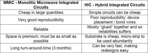
Both implementations MMIC and HIC are cutting edge technologies and they have a good performance, but in our current design has been considered the hybrid implementation due its low cost and because it is easier to build. Furthermore, to build MMIC circuits is needed very expensive and sophisticated materials and machineries, for this reason in an eventual implementation of our design, this option (MMIC) has a low probability to be implemented.
In the design of RF and microwave devices and components, it is very important to have an accurate and sophisticated tool both for the calculations and the simulation. Currently, there are some good tools to perform these activities such as Agilent Advanced Design Software ADS, AWR Microwave Office and others (Alabaster). The tool selected for this work was AWR Microwave Office (MWO) because it offers a friendly environment in comparison with other tools and also due to the availability of licenses at the campus of Polytechnic di Torino.
2. Parameters and requirements
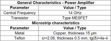
As mentioned at the beginning of this paper, our purpose is to describe a generic process for the design of a power amplifier; however, in this case and to show the rest of the processing in the next sections, the parameters of the current design are shown below in Table 2.
3. Design and Methodology
The first step consists on checking the behavior and the characteristics of the active element, i.e. the MESFET transistor, then the transistor gain and finally the input and output matching networks. In the next sections we make a deeper explanation of these topics.
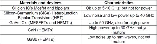
In our design has been used a MESFET transistor due to its availability, but this is not the unique option, in the Table 3, are shown in a brief description the different options according to the materials (Pirola, 2012).
3.1. Checking the stability
First of all, the stability of the transistor needs to be checked. To do that, two conditions have to be verified, the first condition is that the stability coefficient being greater than one (K > 1), where:
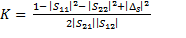 (1)
(1)
The second condition is that the module of the determinant of scattering matrix (S) being lower than 1 (|∆S| <1), where:
 (2)
(2)
All the different S parameters, S11, S12, S21, S22, as well as, the stability coefficient K and the determinant ∆S are computed using MWO.
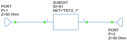
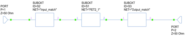
To check the stability it is also useful to have the information provided by the scattering matrix obtained from the transistor MESFET (FET2_1 in simulation). The scattering matrix of the transistor and the different graphs are obtained through MWO. The schematic needed to compute both the matrix S and the determinant is the shown in Fig. 1, where the 50 ohms impedance on both input and output corresponds to the requested values of the input and output matching networks. The schematic shown in the Figure 1, is a starting point of the design and it is suggested in some literature as in (Pirola, Teppati, & Camarchia, 2007) and (Camarchia, Teppati, Corbellini, & Pirola, 2007).
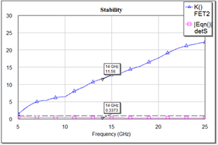
Both, K and |∆S| fulfill with the conditions mentioned above, and their different values in a region of analysis from 5 GHz to 25 GHz are shown in Figure 2.
3.2. Transistor Gain
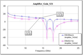
In order to know the behavior of the active element (transistor FET2), it is also suggested to check the power gains, the MAG Maximum Available Gain (the maximum gain GMax), and |S21|, which is the gain when the device is close on both ports with the normalization impedance (50 Ω). Both gains in dB are shown in the Figure 3.
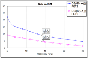
In Figure 3, it can be noted that the device behavior is linear (stability condition) in terms of gain. Now, based on the analysis from Fig. 2 (K > 1 and |∆S| <1) and observing the Fig 3., it is noted that when the device is working in a range of frequencies between 5 GHz and 25 GHz, and of course in 14 GHz, it has a behavior “unconditionally stable”. In addition, Fig. 3 shows that the maximum device gain at 14 GHz is Gmax= 9.206 dB, and |S21|= 4.7161 dB, i.e. S21 < Gmax; at end of design it is expected to get Gmax = S21 at 14 GHz. The maximum power transfer occurs when the generator yields the maximum power, i.e. the input power is the generator (input) available power and the power on the load is the output available power. The maximum power transfer implies power impedance matching simultaneously at the input and output (if this is possible). The maximum operational gain is:
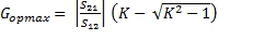 (3)
(3)
Furthermore, to completely understand the behavior of the device, it is convenient to plot the constant gain circles and the stability circles. According to the gain circles, GOP circle (GOP: operating gain - Gamma L) is respect to output, and GAV circle (GAV: available gain - Gamma G) is respect to input, see Figure 4 (Teppati, Ferrero, Pisani, Colantonio & Limiti, 2005).
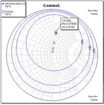
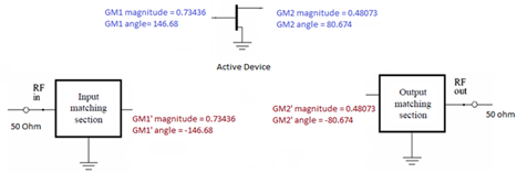
As it is expected, the stability circles (SCIR 1 and SCIR 2) do not appear since the element (transistor) is “unconditionally stable”. Meanwhile in the analysis of the gain circles, it is verified that there is a maximum in the plane ΓG for GAV and a maximum in ΓL for GOP. These maximum values correspond to optimum values ΓG opt. and ΓL opt., It can be noted that MWO is able to directly compute the value of ΓG opt, and ΓL opt.. MWO define these parameters as GM1 (ΓG opt) and GM2 (ΓL opt.). In Table 4, it can be noted the complex values of ΓG opt. and ΓL opt.; these values of GM1 and GM2 expressed in magnitude and angle will be very useful for the design of the matching networks as it will be shown later.
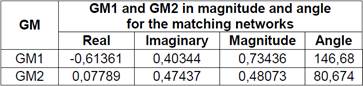
GM1 and GM2 indicate that working with the current active device in a given frequency (e.g. 14 GHz), and considering 50 Ω of input and output impedance, there are only two passive loads, one at the input port (GM1), and the other at the output port (GM2) that ensure the simultaneous match at the two ports of active device (MESFET), hence now the task consists in designing two lossless matching networks.
3.3. Design considerations and simultaneous matching networks
Considering that the design consists of making an amplifier that works with maximum gain, it is necessary to design the corresponding lossless matching networks, remembering that a two-port unconditionally stable system can be simultaneously matched at both ports. In this case, all the power will be transferred from generator (maximum power) to the load ZL, i.e. GOP = GAV = GMAX; in other words, when the device sees GM1 at the input port, and GM2 at the output port, it achieves the maximum gain GMAX (i.e. |S21| = Gmax).
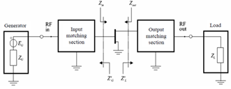
Considering the active device (transistor) and the input and output matching network, the general scheme of the desired amplifier is shown below in Figure 5, (Camarchia, Teppati, Corbellini, & Pirola, 2007).
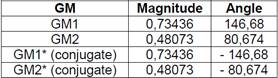
In order to implement the input and output matching networks, it is necessary to work with conjugate values of GM1 and GM2, so as to eliminate the imaginary parts of GM1 and GM2, as it is show in Table 5 and in Figure 6, i.e. the matching network is a conjugate matching of an active two-port device.
When the matching condition is satisfied, S11 and S22 of the amplifier will be zero and |S21| = GMAX. Now, all the considerations to design the matching networks are available, but before, some parameters in MWO have to be configured, as it is done below.
3.4. Design considerations in MWO
The design must be implemented using microstrip lines, whose parameters (substrate and metal) are described in Table 1 and shown in Figure 7.
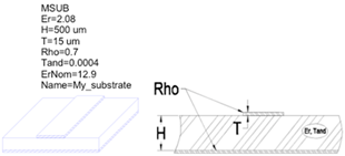
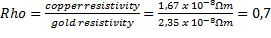
Remembering that resistivity of the metallization (Rho) is normalized to gold, for copper its value is:
 (4)
(4)
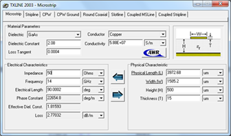
The TXLINE tool of MWO (Figure 8) will be used with the amplifier data to automatically get the width and the physical length for the transmission line. In particular, for this design we considered a fixed width, while the parameter that could change is the physical length.
3.5. Matching networks: Input matching network
In the design of the input and output matching networks we considered not only the microstrip lines, but also a serial short circuit stub, i.e. the input and the output are composed by the transmission lines and the stubs (Raab, Asbeck, Cripps, Kenington, Popović, Pothecary & Sokal, 2002).
The desired values of resistance and reactance are obtained with microstrip lines and short-circuit stubs. The aim at the moment is to couple the input and output networks by modifying certain parameter, in this case the physical length of the line and stub. The modification and all necessary changes in the length do not matter because establishing the goals and using optimizer all changes are performed automatically and then these can be tested using Smith chart or other kind of graphs. In general the scheme of the amplifier looks like as the shown in the Figure 9.
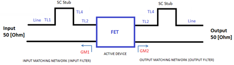
For the design,the width of the transmission line has been considered as a fixed parameter (W= 1585 um) and the variable parameter is the physical length (TL2 and TL4 for the input and the output network, see Fig.9). By means of the optimizer tool of MWO, the best dimensions of the length to satisfy the goals and needs is obtained automatically. The first step is to set the goal for the matching network, in this case the goal is to minimize the S11 (reflection coefficient) in order to transfer the maximum power from the generator toward the load, so, it is set to |S11| < -30 dB and in a range of frequencies between 13.8 GHz and 14.2 GHz (central frequency at 14 GHz), in particular narrow band design has been considered because it is less complex.
Once the goal is established, we have to select the parameters to be optimized (variables). For the input matching network, the physical length of TL2 and TL4 are the parameters to be optimized, then the optimizer is run with the desired values according to the established goal. Furthermore, the size of the elements has been constrained to avoid negative values (Lower=100 um, Upper=9000 um).
Finally, the input matching network (input filter) is obtained using all the elements and dimensions. Its scheme is shown in Figure 10.
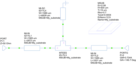
Once the input network has been designed, its operation has to be checked. The S11 parameter in the Smith chart and in a rectangular graph give enough details of the behavior of the input network and the fulfillment of the goal (|S11| <-30 dB), see Figure 11.
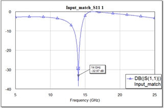
Analyzing Fig. 11, it can be noted that the design of the input matching network has been completed successfully, since |S11| dB is lower than the fixed goal (|S11| = -32.97 dB) and the reflection coefficient is 0 (real= -0.01664, imaginary=-0.015).
3.6. Matching networks: Output matching network
As before in this case, the goal is |S11| < -30 dB, and the variables to optimize are TL2 and TL4. Following the same procedures as in the input matching networks, the results obtained are shown below, see Figure 12.
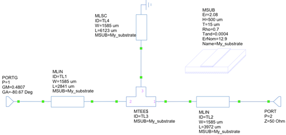
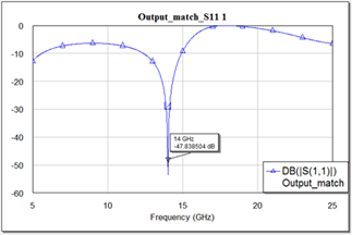
Analyzing Figure 12 and Figure 13, it can be concluded that the design of the output matching network has been completed successfully, since |S11| dB is lower than the fixed goal (|S11| = -47.838504 dB) and the reflection coefficient is 0 (real= -0.0006447, imaginary=-0.004004).
4. Results
Up until this point, both networks, input and output, are designed and they need to be combined with the active element. The whole amplifier is shown in Figure 14.
Of course, and as stated above, it is necessary to evaluate the behavior and the performance of the amplifier in terms of reflection coefficient and gain.
Analyzing the graphs of Figure 15, it can be concluded that the objective of designing an amplifier at 14 GHz with maximum gain has been fulfilled. Finally, appropriate lossless matching networks help to build amplifiers providing maximum power (GMAX), as illustrated in Figure 15 that shows that S21 = GMAX at 14 GHz and S11 and S22 (input and output reflection coefficients) are very small values (under -30 dB).
4.1. Layout of the amplifier
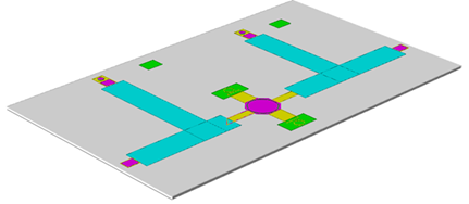
Having designed the amplifier, is very easy to get its layout. MWO gives the possibility to plot 2-D or 3-D layouts, with the option “layout”. Taking in mind that the amplifier contains an active device (transistor), it is necessary to consider a power supply in the design (BIAS), and capacitors in the input and in the output to block the DC component (Camarchia, Moreno, Pirola, Quaglia & Wegeland, 2013), so the final implementation of the amplifier looks like the shown in Fig. 16, (Kawai, Ohta & Enokihara, 2010).
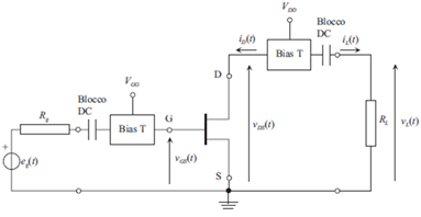
In order to obtain the final layout, the scheme will change a little due to the association of the different elements (transistor, capacitors). The bias capacitor value was calculated based on the consideration about the work frequency, taking into account that the capacitor should act as a short circuit at 14 GHz of frequency, and that:
 (5)
(5)
The value of the capacitor is 22 pF and the amplifier with all additional elements is the shown in the Figure 17, it is shown a layout in 2-D and 3-D.
5. Conclusions
Analyzing all the graphs above, we conclude that the objective of designing an amplifier at 14 GHz with the maximum gain has been fulfilled. With the support of MWO, the processes were achieved in a more simple way, but all the processes need to be performed in the correct order and with coherence to obtain the best results. The steps and procedures above could be used in other designs since the principles and the considerations done for the design wew generic and not oriented to a particular frequency or transistor. A correct preliminary analysis of the matching networks is very useful and necessary in order to obtain the maximum available gain of the transistor. A plenty of choices are possible to match the impedance of the transistor and to choose the correct one it is necessary to consider the physical length and the final size of the amplifier.
Microstrip technology provides tremendous advantages regarding the design. Some elements such as amplifiers, matching networks, couplers, diplexers and a lot microwave devices could be implemented using microstrip technology, and this technology has some advantages , which are mainly the little space these devices need and their reduced weight.
The traditional design is a good starting point to have an idea of the goals and the expected behavior of the amplifier; however, the active element i.e. the transistor, the parameters and the characteristics are totally different. Indeed, the design itself is different, so all the steps described above are a suggested path to follow in the design of power amplifiers or other RF devices.
Currently, software tools such as AWR Microwave Office or ADS are, without doubts, very helpful, but furthermore it is needed to have a clear idea of the goals, purposes and application of the design. With a suitable methodology and fundamentals it is possible to start with the basics and to continue to more complex systems.

