


 Español (pdf)
 Articulo en XML
 Referencias del artículo
 Enviar articulo por email
 Citado por SciELO
  Similares en
SciELO
Similares en
SciELO 
 Permalink
Introduction
Multibeam and beam-scanning antennas are crucial to modern communication systems such as Direct-Broadcast Satellite (DBS), Multipurpose Radar, multiple beam antenna for mobile communications. Talking about these systems is talking about the smart antennas and indirectly of multibeam systems the require wide-angle coverage with very directive beams. Multibeam and beam-scanning antennas are implemented using multiple antennas to create several beam patterns in different directions, either as beam switch or continuous beam terminated in a sophisticated signal processor, which can adjust or adapt its own beam pattern in order to emphasize signals of interest and to minimize interfering signals (Abdelghani et al., 2012a, Abdelghani et al., 2012b, Bialkowski et al., 2008, Moscoso-Mártir et al., 2014).
Beamforming networks are a great solution to generate several beams with great directivity and good bandwidth, they have been classified into several ways, it was reported in the applications cited previously, so to facilitate our learning it has been divided into 3 groups according to their applications: based on transmission lines (Network BFNS), based on quasi-optical lenses (Quasioptical BFNS) and based on digital data processing networks (digital BFN), (Lo & Lee, 1988, Hansen, 2009, Hall & Vetterlein, 1990, Josefsson & Persson, 2015).
All these solutions offer multiple-beam or beam-scanning capabilities by selecting one or several input ports, or mechanically displacing a moving feed, but the Butler matrix and Rotman lens are widely used since they can achieve a large number of switched beams using well-known design algorithms.
In the present research, three microwave circuits to generate multiple beams are proposed, each proposed beamforming network have been designed for a different resonance frequency. This paper is described in 3 sections, in the first section a 4X4 Butler Matrix design at 2.45 GHz is described in detail, in the next section a Rotman lens at 5.8 GHz is developed, and it is compared with a slots array designed with Substrate Integrated Waveguide (SIW) technology, which is described in section 3, finally the conclusions are presented in the last section.
Butler Matrix
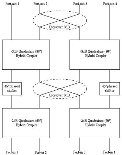
A 4 x 4 Butler Matrix is designed using four -3 dB Quadrature (90 degree) Hybrid Coupler, two 0 dB Crossovers Coupler and two 45 ∘ phased shifter (Nachouane et al., 2014), it is shown in figure 1. The prototype has been optimized at the center frequency of 𝑓=2.45 GHz in WiFi applications (IEEE 802.11b/g/draft-n), with a characteristic impedance of 𝑍 0 =50Ω. The material considered for the design has the following characteristics: Roger 4003C with 𝜖 𝑟 =3.38, height ℎ=0.813𝑚𝑚, Tan (𝛿)=0.0027.
2.1 -3 dB Quadrature (90°) Hybrid Coupler
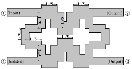
Quadrature hybrids are 3 dB directional couplers with a 90 ∘ phased difference in the outputs of the through and coupled arms. In the design of -3 dB Quadrature (90 degree) for Hybrid Coupler. The dimensions of the transmission lines are shown in table 1, these values have been obtained from the equations provided in Pozar (2011) and Balanis (2005).
Table 1: Hybrid coupler dimensions.
| Impedance | Lenght | Width |
|---|---|---|
| 50 Ω | 18.7438 mm | 1.84139 mm |
| 35.35 Ω | 18.3137 mm | 3.1044 mm |
A generic hybrid coupler was designed based on the values specified in table 1, however the technological advancements require miniaturization of the systems to optimize space and compact structure, therefore each of the elements of the hybrid coupler have been divided into five equal segments, as a overlapping transmission lines resulting in a size reduction 30%, it is shown in figure 2.
2.2 Butler Matrix proposal
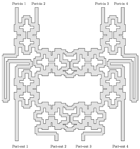
To build a Butler Matrix we have relied on the criterion of figure 1, where it requires hybrid couplers, crossover couplers, and phased shifters. Crossover couplers are known as couplers to 0 dB, these are an efficient way for crossing two transmission lines with minimal coupling between them, the simplest form of designing such devices is by means of a connection of two hybrid couplers 90 ∘ . Additionally, it is important to considerate the symmetry properties (Kholodniak et al., 2000). In figure 3 is depicted the proposal Butler Matrix; to design the phased shifter we have decided to change the length value, this because a length at 45 degrees is too short to use, therefore, the new phased shifter length was calculated with an angle at 405 degrees. The resulting size was 7.8cm x 7cm, which corresponds to the proposal Butler Matrix.
The return loss and phase difference between the output ports of the Butler matrix (see figure 4), give us to identify that the proposed design is resonating at 2.45 GHz of frequency with a bandwidth about 28%; i.e. it has a working window of approximately 500 MHz.
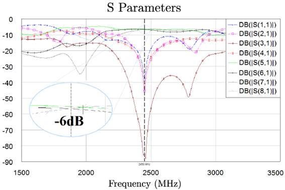
Figure 4: S parameters of the optimized Butler Matrix (1-4 are input ports and 5-8 are output ports).
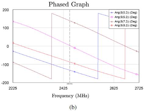
In table 2 is shown the variation of the phase angle between the ports of entry ( 𝑃 𝑖𝑛 1 , 𝑃 𝑖𝑛 2 , 𝑃 𝑖𝑛 3 , 𝑃 𝑖𝑛 4 ) with respect to the output ports ( 𝑃 𝑜𝑢𝑡 5 , 𝑃 𝑜𝑢𝑡 6 , 𝑃 𝑜𝑢𝑡 7 , 𝑃 𝑜𝑢𝑡 8 ) of the designed Butler matrix. In figure 4, the phase diagram is obtained; for entering input port 1 is shown, which presents an angular variation of -45 degrees. On the other hand, figure 4 depicted the second case, input port 2, describes the angular variation of 135 degrees. Based on both results, we could build a four elements array antenna to increase directivity.
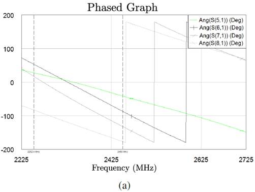
Figure 5a: Phased output ports of the Butler matrix optimized. (a) Output ports with respect to the input port 1
Rotman Lens
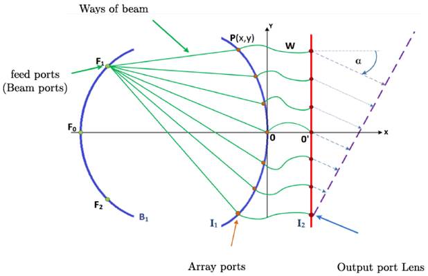
A Rotman lens is a device that uses the spread of an injected signal into the gap between two parallel metal plates to achieve the condition of a linear phase distribution in the output ports of the lens. The geometry of the metal plates and the length of the output cables are obtained using the geometrical optics model.
In practice, this condition is only true for the ports on the perfect focal points, whereas for the other ports located along focal arc, the phase variation will be approximately linear, resulting in phase errors (optical aberrations) that affect the performance of the lens.
The outputs of the lens will be used to feed a linear antenna array in order to change passively the phase distribution at the input ports of the array. By controlling the phase shift in the array ports, it is possible to direct the radiation pattern of the antenna toward a predefined direction (see figure 6 ).
A prototype of a Rotman lens using a NELTEC NY9220 substrate was designed and simulated. The dielectric substrate has a permittivity of 2.2 and thickness of 0.127mm. The parameters used in the design of the lens are described in table 3.
Table 3: Rotman lens parameters.
| Parameter | Value |
|---|---|
| Central frequency 𝑓 0 | 5.8 GHz |
| Bandwidth (BW) | 4 MHz |
| Maximum scan angle (Ψ) | 30 0 |
| Maximum focal angle (𝛼) | 30 0 |
| Output ports (antennas) | 11 |
| Distance between output ports | 1.955cm |
| Input ports (beams) | 7 |
3.1 Rotman Lens design using the geometrical optics model
In general, the design of a Rotman lens should follow a systematic procedure to obtain the expected results. A standard design procedure consists of definition of the lens specifications, this is proposed in two stages.
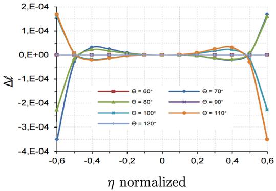
In the first stage are defined: maximum scan angle, maximum focal angle, number of beams, return losses, phase errors, amplitude errors, bandwidth, efficiency, among others. In order to determine the length of the normalized aperture of the lens ( 𝜂 𝑚𝑎𝑥 ), the path length errors for different pointing angles were evaluated (Rotman & Turner, 1963). Trough figure 7 it is possible to verify that, to get an error less than 5x10⁻⁴, 𝜂 𝑚𝑎𝑥 should be less than 0.5. That value will be taken as the maximum value for the normalized aperture.
In the second stage, the data contained in table 3 and the geometrical optics model were used to calculate the coordinates of the output ports of the cavity, and the length of the lines between these ports and the lens output ports (see figure 6).
The length of the central focal point (the width of the lens), can be calculated using the equation (1), where 𝑁 𝑒 = number of antenna elements, 𝑑 = distance between elements, 𝜂 𝑚𝑎𝑥 =0.5and 𝜖 𝑟 =2.2 is the permittivity of the substrate.
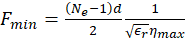
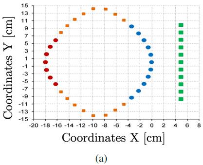
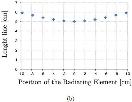
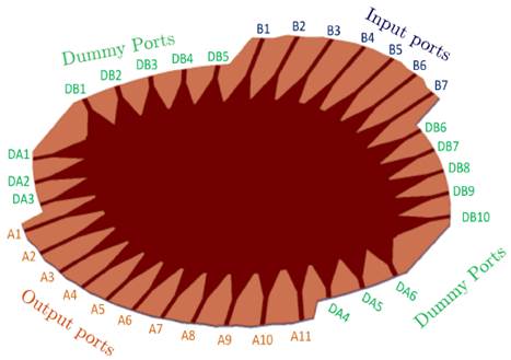
The positions of the lens elements are depicted in figure 7: the red dots correspond to the beam ports (input ports), the blue dots are the array ports (inner ports), orange squares are the dummy ports and the green squares are the output ports (linear array). The lengths of the lines connecting the array ports with antenna ports is plotted in figure 7.
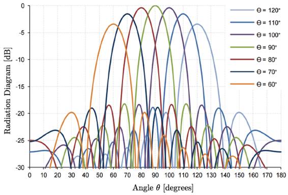
Once the geometrical parameters have been calculated, the two-dimensional model (Lo & Lee, 1988) was used to evaluate the performance of the lens. Radiation patterns for different pointing angles are presented in figure 9. The beams are pointing in the desired directions and the Side Lobe Level is better than 16 dB for all beams; furthermore, the nonexistence of grating lobes can be verified.
3.2 Ports and connection lines
An important aspect to consider is the proper design of the transitions between input/output ports and cavity. For the design of ports, it is necessary to calculate the value of the microstrip line considering that the characteristic impedance 50 Ω, the next step is increase gradually the width (taper) for the purpose of to vary gently the impedance characteristics until are similar which presents the interface between line and parallel plate cavity (Musa & Smith, 1986; Musa & Smith, 1989). Another aspect to consider is the phase center of a microstrip port, ports of the lens should be located so that its phase center coincide with the points calculated in figure 8a and figure 8b, otherwise, errors will occur in the phase of the output signals that can cause unfocused lens. On the other hand, Rotman equations do not define the geometry of the side walls, which connects the focal arc with the array lens arc. The side walls can be designed according to any geometrical shape. In this type of designs, the energy reflected on the walls, returns to the lens body, causing additional side lobes, and it can cause coupling between ports (Rausch & Peterson, 2005). In that reason, in implementations with microstrip or stripline technology, the absorption conditions usually are achieved by placing dummy lenses ports terminated in matched loads along the side walls (see figure 10).
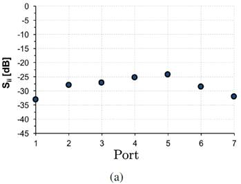
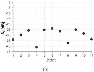
To avoid direct connections between the loads matched resistances and the mass plane, a 𝜆/4 stub length terminated in an open circuit is used. In figure 11a and figure 11b, the reflection coefficients of the input ports and output ports of the lens are plotted. The coefficients are calculated at the center frequency of 5.8 GHz. It shows that for all ports the parameter is less than -20 dB.
Slot Arrays Antenna with Substrate Integrated Waveguides
A Slot Arrays Antenna with Substrate Integrated Waveguides (SIW), is designed by placing two rows of metalized holes in a dielectric substrate, where, 𝑑 = holes diameters, 𝑏 = space between them and the 𝑤 = spacing between the rows are the physical parameters required for the design of the guide. A SIW guide can be modeled using a classic rectangular waveguide, so all design procedures and developed the theoretical basis for rectangular guides are directly applicable to SIW guides (Deslandes & Wu, 2006). The parameters are shown in table 4.
4.1 Slot antennas design
Given the geometry of SIW guides, the slots are placed in the wide face of the guide and parallel to the axis of symmetry. The slots have been shifted an 𝑢 distance from the axis so that cut the current lines of the fundamental mode and to radiate too; this distance allows to control the power level radiated by the slot.
For the design, 5 resonant array with axial feed are used, so the end of the guide is shorted and the last slot will be at a 𝜆/4 short distance. The other slots are separated 𝜆/2 distance between them, and they are located alternately with respect to the longitudinal axis to compensate for the 18 0 ∘ phase produced by the standing wave generated inside the guide.
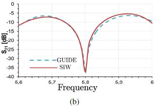
In table 5 are shown the initial values of the group of slots obtained through (Johnson & Jasik, 1984; Farrall & Young, 2004), in figure 12a the linear array are represented of slot with SIW guide used for simulations, in figure 12b are describe a comparison of S parameter of rectangular guide and SIW guide array.
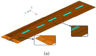
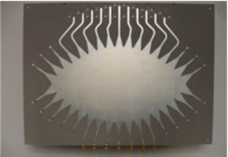
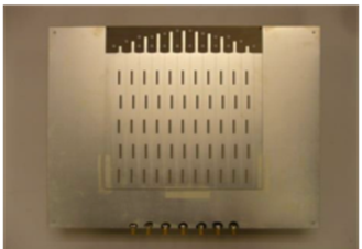
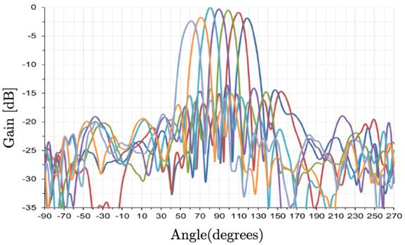
In order to implement the antenna, it is necessary to design a transition between microstrip lines (2 different layers) for obtaining a good bandwidth and also easy to build, in figure 13a is shown the proposed prototype with Rotman Lens, figure 13b shows a prototype with SIW guide, besides in figure 14 are shown the measured radiation patterns of multibeam antenna prototype.
Conclusion
Thanks to the design and simulation of the elements of a Butler matrix as hybrid couplers, cross couplers and phase shifters, we achieved obtaining a new model to create a forming network beam, which can serve for antenna array used in applications WiFi. The developed model has the same properties and characteristics of a conventional Butler matrix, furthermore, it has succeeded reducing size up to 7.8cm x 7 cm; these dimensions represent only the 40% of a conventional design.
It was possible to design a beam forming network using a Rotman lens for a frequency of 5.8 GHz, this design could be performed through two types: based on conventional port and SIW guide ports, these results has been demonstrated through experimental procedures.

