


 Spanish (pdf)
 Article in xml format
 Article references
 Send this article by e-mail
 Cited by SciELO
  Similars in
SciELO
Similars in
SciELO 
 Permalink
1 Introduction
Actually the technology of semiconductors has a fast development with an improvement in the reliability and quality of its components. The Power MOSFET transistors have their parameters of quality, which can be identified on datasheets of manufacture (Bajenescu & Bazu, 1999).
The Power MOSFET device, called MDmesh (Multiple Drain mesh), permits the best performance in the power management, reduction of the size of the package, and the same conduction losses fabricated with a standard technology (Saggio et al., 2000). The Power MOSFET’s of ST’s MDmesh K5 series had characteristics for increasing the efficiency in applications such as LED lighting, metering, solar inverters, 3-phase auxiliary power supplies, and welding (STLife-Augmented, 2017).
The high lead (Pb) soldiers for power semiconductor devices provide good heat dissipation of typically 35 W/mK, is ductile and exhibits desirable thermal expansion properties that tolerate the silicon (4.2 ppm/K), to avoid joint failure due to thermal cyclic stresses [Manikam et al., 2013]. In extreme cases, too little solder may result in voided or open circuits and too much solder may result in solder balling or short circuits (DirectFET-Technology, 2017a). The void is defined such as a blow hole in the solder joint or non-conductive cavities within the soldered joint and their excessive presence poses a significant reliability risk. The IPC-7095 standard specifies a maximum allowable voiding area of 25% (Dusek et al., 2013; Bu et al., 2016). The interconnect solder board joint-to-board is influenced for the pad technology, the dimensions, metallization, and layout (DirectFET-Technology, 2017b). The volatile compounds from paste solder can be evaporated by the soldering process and gaseous components tend to leave the molten solder and some remain inside the solder and create voids (Bu et al., 2016). The electronic assembly of semiconductor devices can have joint solder void problems that will influence not only the reliability of the solder joint but also the electrical, mechanical and thermal properties of the joint (Ruifen et al., 2014). Additionally, the effects of the void on the electrothermal behavior of Power MOSFET, which reduces the ability of the die-attach solder layer to conduct heat from the silicon junction to the heat spreader, are a reason for their study using scanning acoustic microscopy, x-ray, and TEM techniques (Katsis & Vanwyk 2006; Tran et al., 2017b; Kim et al., 1999). The scanning electron microscopy has been able to show the inner structure of field-effect transistors in order of nanometers (Tulevski et al., 2006). The electron microscope has permitted the study of the inner cross-section of MOSFET for modelling via finite volume simulation and the voids effects inside the solder joints can be correlated to the common approach of effective thermal conductivity (Fladischer et al., 2018). Actually, there are studies for avoiding the voids on Power MOSFET’s as well as the methods for the optimization of the join soldiers and the procedures for their evaluation (Tran et al., 2017a; Wild et al., 2017).
The x-ray technique is a method for determining solder voids, joints, bridging, missing parts, trench structures by analyzing the exposed silicon area to improve the performance of devices. However other defects such as broken solder joints are not easily detectable by x-rays (Ruifen et al., 2014; Saxena & Kumar, 2012; DirectFET-Technology, 2017b). The x-ray method can detect some types of voids such as macrovoids with a diameter varying between 100 μm and 300 𝜇m and microvoids with a diameter below 50 𝜇m (Lang, 2017; Bu et al., 2016).
The x-ray scan and simulations of voids on the MOSFET grid with their physical and thermal parameters have an impact on the operation of the device considering that corner voids are more dangerous than centre defects located below the center of a MOSFET chip and the voids spreading on the grid mesh solder which have less impact on the operation of the MOSFET (Chen et al., 2008).
Currently, there are commercial software packages incorporated in computer tomography equipment for x-ray inspection, software for statistical analysis, algorithms for improving void detection and freeware for the manual analysis of voids (GEInspection-Technologies, 2017; Wild et al., 2017; Said et al., 2010; Easton et al., 2008).
There are processing image techniques for automated void defect detection for poor contrast x-ray images which permits contrast enhancement and eliminates the false voids while true voids are not significantly affected (Ruifen et al., 2014).
Nowadays the image processing tools enable fast and accurate void segmentation in the die-attach regions on power transistor for means of X-ray monitoring of imperfect power transistor die soldering, permitting the determination of the most common void parameters such as void area, void distribution and shape roundness (Sesek et al., 2019).
2 Methodology
The investigation was made using a Power MOSFET (N-channel STP20N95K5, STMicroelectronics) and using the SEM method as a preliminary technique and microtomography procedure as an NDI method.
2.1 Scanning Electron Microscopy with Energy Dispersive Spectroscopy
The unpacking of the Power MOSFET was carried out by applying a heat gun to remove the external package, according to the manufacturer’s recommendations. The preheating rate was 2 ∘ C per second until a temperature of 12 5 ∘ C, was reached. Afterwards, the temperature was increased to 22 0 ∘ C during 6 seconds for unpacking the device, considering 26 0 ∘ C is the maximum peak welding temperature for this device (STMicroelectronics, 2019), then the interior of the device was corroded using hydrochloric acid diluted at 60% on distilled water (figure 1).
Scanning electron microscopy with energy dispersive spectroscopy (SEM-EDS) for elemental analysis and surface morphology of solid materials, the SEM generates the microphotographs of the roughness, topography of the sample; the elemental analysis is obtained by EDS, which facilitates the elementary quantification of the sample (figure 2) (Holt & Joy, 1989).

Figure 1: Inner structure of Power MOSFET after unpacking procedure. (a) The current Power MOSFET. (b) Power MOSFET without package, (1) Metallic drain, (2) Silicon layer, (3) Lead solder layer, (4) External package.

2.2 Microtomography Laboratory
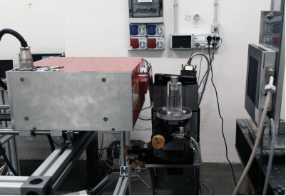
The micro Computed Tomography (𝜇-CT) scan was carried out at the Microtomography Laboratory at the University of Calabria, Italy. As in figure 3, the Microtomography experimental station consists of three precision optical tables (Thorlabs model B6090B), equipped with a microfocus X-ray source (Hamamatsu L12161-07) with a voltage range from 0-150 kV and a variable focus mode which can reach 5 𝜇m at 4 W on a small focus operation. The motorized structure consists of two motion cradles (PI model WT-90), a rotator (PI model PRS-110), and two motors for linear translation (models PI LS-180 and LS-270). It uses a flat panel detector (Hamamatsu C7942SK- 05) with a maximum value of 150 kVp and a resolution of 5.4 Mpixels (pixel size 50 x 50 𝜇m). The control system permitted the sample-under-test (SUD) moving, using five high precision stepper motors; the image acquisition by means of a flat panel detector, subsequently made the 2D reconstruction using N-Recon and 3D image reconstruction using the ImageJ freeware tool.
2.3 Microtomography Technique
The microtomography technique uses a cone-beam geometry which is advantageous for obtaining directly reconstructed 3D images from a set of 2D projections recorded by a detector (Machin & Webb, 1994; Turbell, 2017). The reconstruction process was made using phase retrieval to obtain a cross-section 2D image from the sample and resulting in a 3D dataset (Vlassenbroeck et al., 2007).
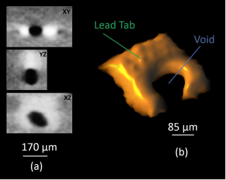
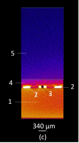
The 3D X-ray 𝜇-CT provides a powerful non-invasive alternative solution for these problems associated with failure analysis (Pendleton et al., 2008). The microtomography permits NDI of some electronic devices without causing damage to them and allows their subsequent utilization. The cone beam 𝜇-CT uses a variable range of energies and resolutions of a few microns, which permits the inspection of the inner structure of the electronic device and gives a fast look inside the 2D projections, which following their reconstruction, allows a 3D rendering from the object to be obtained a 3D rendering from the object (Hanke et al., 2008). Figure 4 depicts a single void of lead solder and figure 5 shows cross-section of Power MOSFET after NDI inspection.
Before the 𝜇-CT test was obtained, the optimum magnification, energy and position of the Power MOSFET was determined and the setup of the 𝜇-CT station for acquiring the best contrast. The Power MOSFET was placed on suitable a sample holder while verifying which package area was to irradiated for at least 15 % of photon transmission. The acquisition parameters were 140 kV, 71 𝜇A, 2000 ms of exposure time, 0.2 mm rotation step and 6 of magnification.
The 2D reconstruction was obtained by using the NRecon software (free-ware version), the standard reconstruction parameters were: smoothing factor = 4, beam hardening correction = 10 % and ring artefact reduction = 10.
The 3D reconstruction involved routines of ImageJ software, a FTT band-pass filter was applied for defining the spatial frequency domain of lead solder 3D image and final application of a segmentation procedure by selecting a grey level range.
2.4 Image Processing
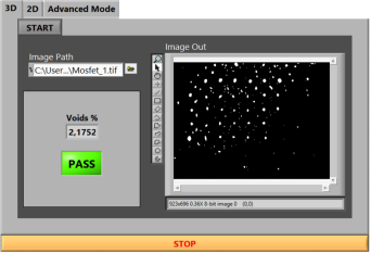
The software was developed over LabView platform using IMAQ Vision Library (National-Instrument, 2017), it was developed for 3D images and 2D planar radiographs (figure 6 and figure 7) respectively, permitting in real-time analyze the voids. Before acquisition was verified manually the region of interest of Power MOSFET was perpendicular to the flat panel sensor.
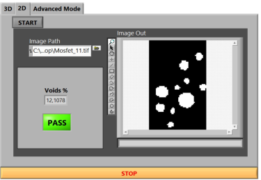
As the program accepts an 8-bit image at a time, the first step was to acquire a 3D image on a TIFF format of the voiding area (figure 7). After the acquisition was completed a template for the calibration of the image using a real scale was used (figure 10), in order to calibrate the distortion regions and fix the correct angle and its dimensions. The image calibration involved extracting the grid features by selecting the square form and threshold parameters for each image and looking for dark objects using the background correction method with a kernel size of 56 x 56, the region of interest was 1 x 1 and the valid dot area of 10 - 5000; the valid circularity was 0.8 - 1.2 origin calibration axis and ignoring any objects with regions that touched the chip’s borders. Specified grid parameters were x: 680 𝜇m, y: 680𝜇m and the distortion model was based on the polynomial K1 model, which permitted a review of the calibration results as being acceptable, with a distortion of 0.107 % and a standard deviation of 0.04. The calibrated image was filtered using a convolution linear filter; the calculations were made using a floating point number with a 7 kernel dimension. After, the automatic threshold detection permitted the voids detection and extracting their quantitative information such as perimeter, area, and mass center. As in figure 8 shows the graphic user interface for the advanced mode menu, which permits the calculate the number of macrovoids and microvoids, the voids percentage respect of the total area, the average mass center, the maximum and minimum void measure, and the histogram that represent the percent of voids respect their area.

3 Results
Figures 9-10 depict the image of the lead solder and illustrate the calibration template used for processing of the image, respectively. Figure 11 shows the resulting lead solder image following the calibration procedure adjusted to real scale and tilt. The solder layer and its voids are better depicted after convolution filtering in figure 12, and figure 13 shows the automatic threshold for voids over lead solder. The selection and improve filter is a crucial point for voids detection. After the test the device passed the quality control with approximately 2.2 % (figure 6), where the microvoids had no considerable impact on the overall percentage of defects (0.3 % microvoids vs 99.68 % macrovoids) (figure 8). Figure 15 shows the graph of the voiding mass center for each void of lead solder, figure 16 depicts the graphic of the macrovoids mass center and figure 17 illustrates the microvoids mass center on the solder layer.
The program was developed for calculating the percentage of voids based on its pixel value, has obtained a percentage of 2.195 % although using real measurements from image calibrated template the percentage was of 2.175 %. Verified the importance of calibrated image for obtaining more exact results due to calc using pixel value can truncated or rounded some voids results.
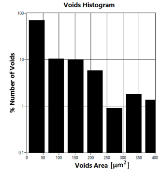
Figure 18(a) corresponds to the 2D radiograph of the source contact from a Power MOSFET with DirectFET technology (DirectFET-Technology, 2017b), whereas figure 18(b) shows the result after thresholding with a lower value of 82 and an upper value of 255 ( figure 5). The amount of voids obtained was 12.11 %, a result which is very similar to that obtained by the manufacturer with values in the range of 12-13 %. Figure 19 shows the void’s histogram representing the void statistics by area.
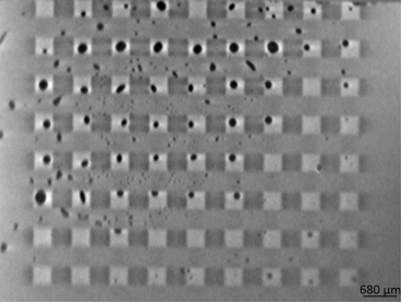
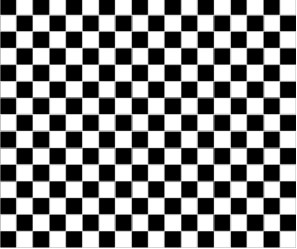
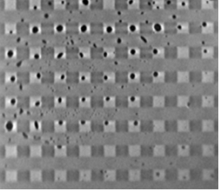
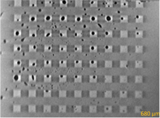
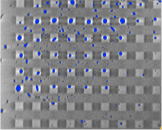
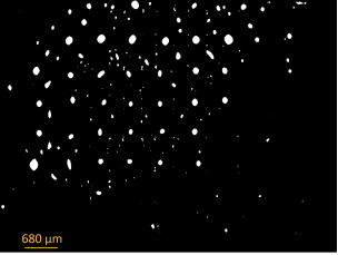
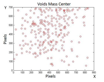
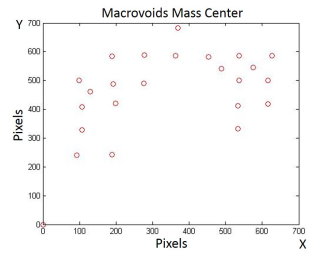
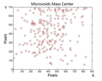

Figure 18: 2D Radiograph of Power MOSFET - Source Contact. (a) Left Source Contact. (b) Threshold image.
4 Conclusions
The methodology used permitted for the first time the non-destructive inspection of the inner structure of STP20N95K5 Power MOSFET using the microtomography technique for quantifying macro and microvoids and their location on the lead solder by using a software on LabView. The 2D images generated as a result of the microtomography technique permitted a 3D reconstruction of the device and showed in detail its inner structure, specially the solder layer and their voids through 3D image segmentation. The methodology applying in this research can be used for high-quality production of devices even further, in-line inspection, however, the time of the inspection is long.
The results demonstrated which the Power MOSFET manufactured by STMicroelectronics have high standards of quality due to the low impact of voids its operation (≈ 2.2 %), considering the maximum permitted is 25 %.
This work demonstrates that the 𝜇-CT could be employed in industrial applications as the quality conytrol method and for characterization of the constructive process. Therefore, the quantitative results obtained with this software can represent a good guide to designing innovative devices.
Future work can include improving this sensitive non-destructive inspection system by directly scanning the voids in the 2D planar images.

